Redesign Online Circuits
How to start your design from one or multiple open source Eagle files online, and redesign to make it easier to fabricate
There are an infinite number of circuits and combinations of circuits that you might make, so it is impossible for this guide to cover what you're circuit will need (or not need).
However, this guide will use a simple circuit to show you the basic steps you will always take when starting a design from open source circuits.
This guide assumes you have gone through the previous Eagle tutorials, on both schematic and board design.
Finding an Online Design
Companies like Adafruit and Sparkfun share their designs online. This makes it possible to first breadboard and test a circuit using their products, and then to use their designs to make a custom PCB (amazing!).
The same process described below can be done with any open source company or design files. Github is the most common place for open source Eagle files, so you can just go straight there and search.
(For example) I'd like to make a PCB using the ESP8266, so it can be WiFi connected.
Adafruit has a few PCBs that use the module described in the recommended parts page. Looking through their products, it looks to me like the HUZZAH board.
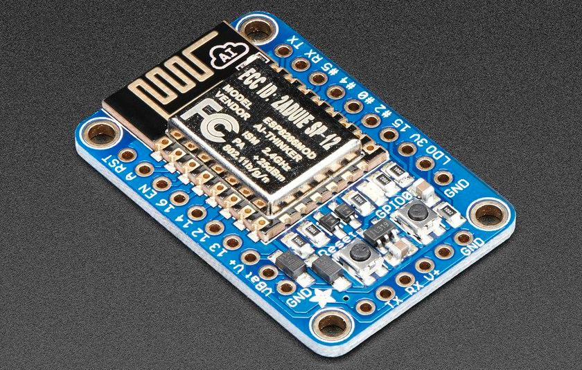
On Adafruit's product page for the HUZZAH, scroll down near the bottom of the page, and there is a link to the tutorial on using the HUZZAH breakout board.
Whenever researching a new part, read through the entire documentation to make sure you fully understand how to use it, and if it is the right part for your project.
Adafruit always includes a link to their Eagle files at the end of their tutorials in the Downloads section. They will link to a Github repository with their PCB files.
Removing Unnecessary Parts
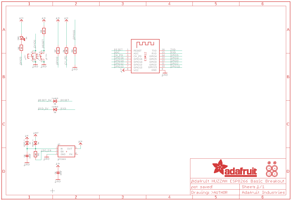
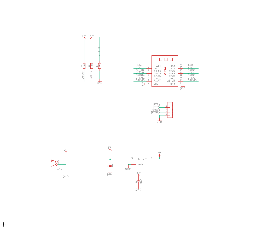
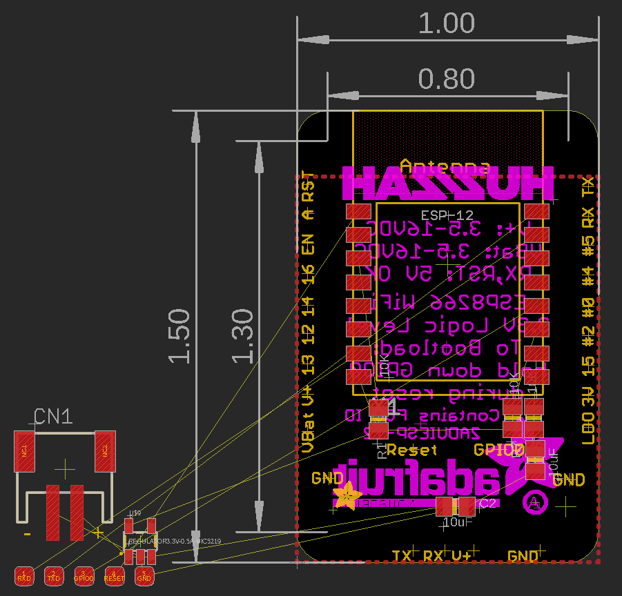
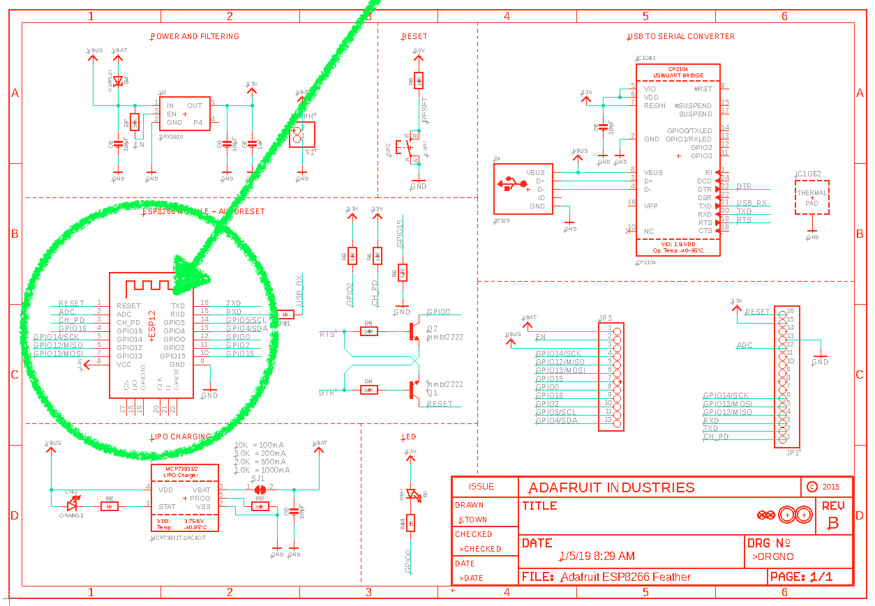
Open the HUZZAH Eagle files and take a look at the schematic.
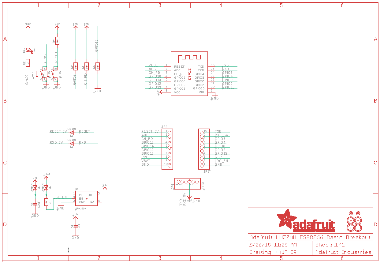
It's a fairly simple schematic. The ESP8266 is in the top right, and most of its pins are connected to the headers on the bottom right.
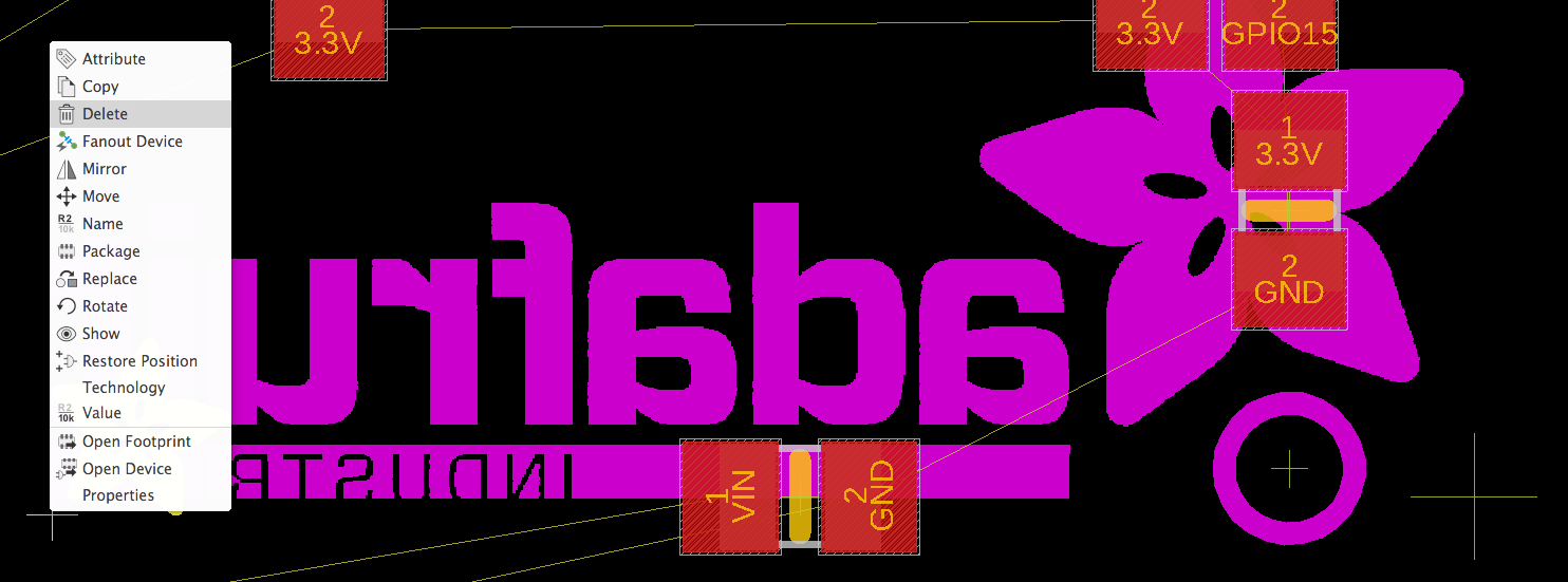
My final PCB will not need all of those headers, because it will be a contained project. So, we can delete all the headers.
There is a regulator on the bottom left, converting a 3.3-12.0 volt input to the 3.3 volts that the ESP8266 can use.
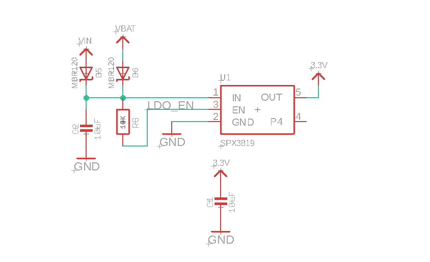
There are also some protection diodes, which prevent battery and USB voltage sources from touching each other. Because I know the my project will have only one voltage source, I think I am safe to delete those protection diodes.
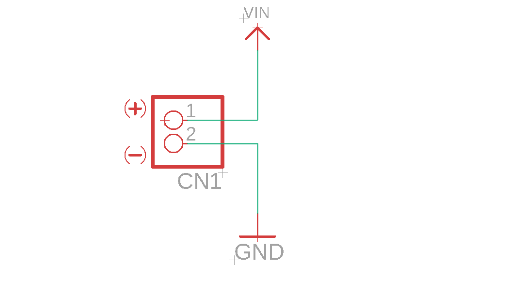
I will also only use the Vin name for the input voltage, and delete the Vbat symbol, because there will be only one power source.
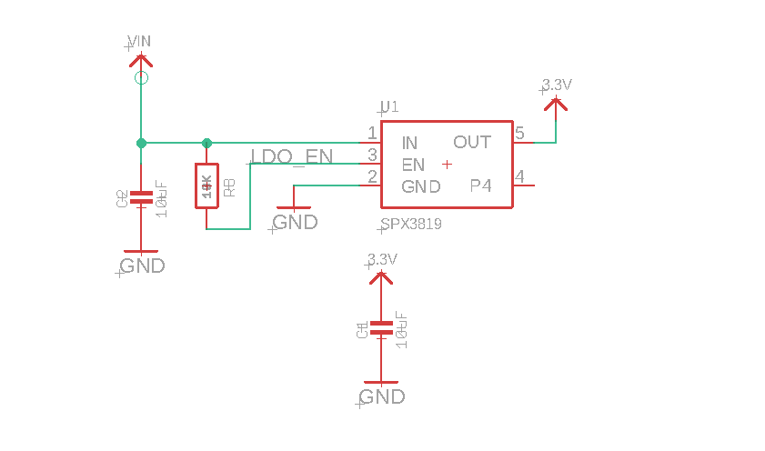
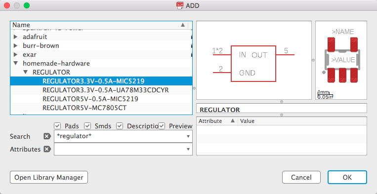
Now I have two options: 1) use the same regulator Adafruit uses, and order it online, or 2) replace this regulator with a regulator I already have.
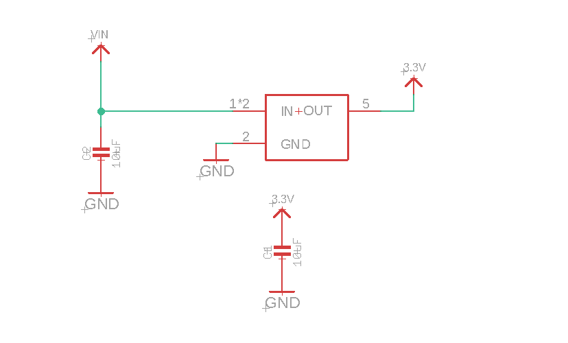
I'm going to go with option number 2, so I don't have to order a new one. I'll use the MIC5219 3.3 volt version.
Directly above the regulator, there are two protection diodes. Adafruit is using these diodes to protect the ESP8266 from a 5V serial adapter.
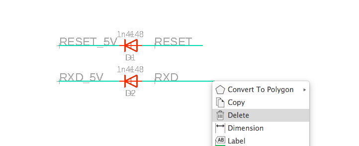
I am going to use the FTDI Friend to program my PCB. This USB to serial converter has the option to run at 3.3V, so I will not need these protection diodes. The adapter's voltage and my project's voltage will be very close, so there is no danger.
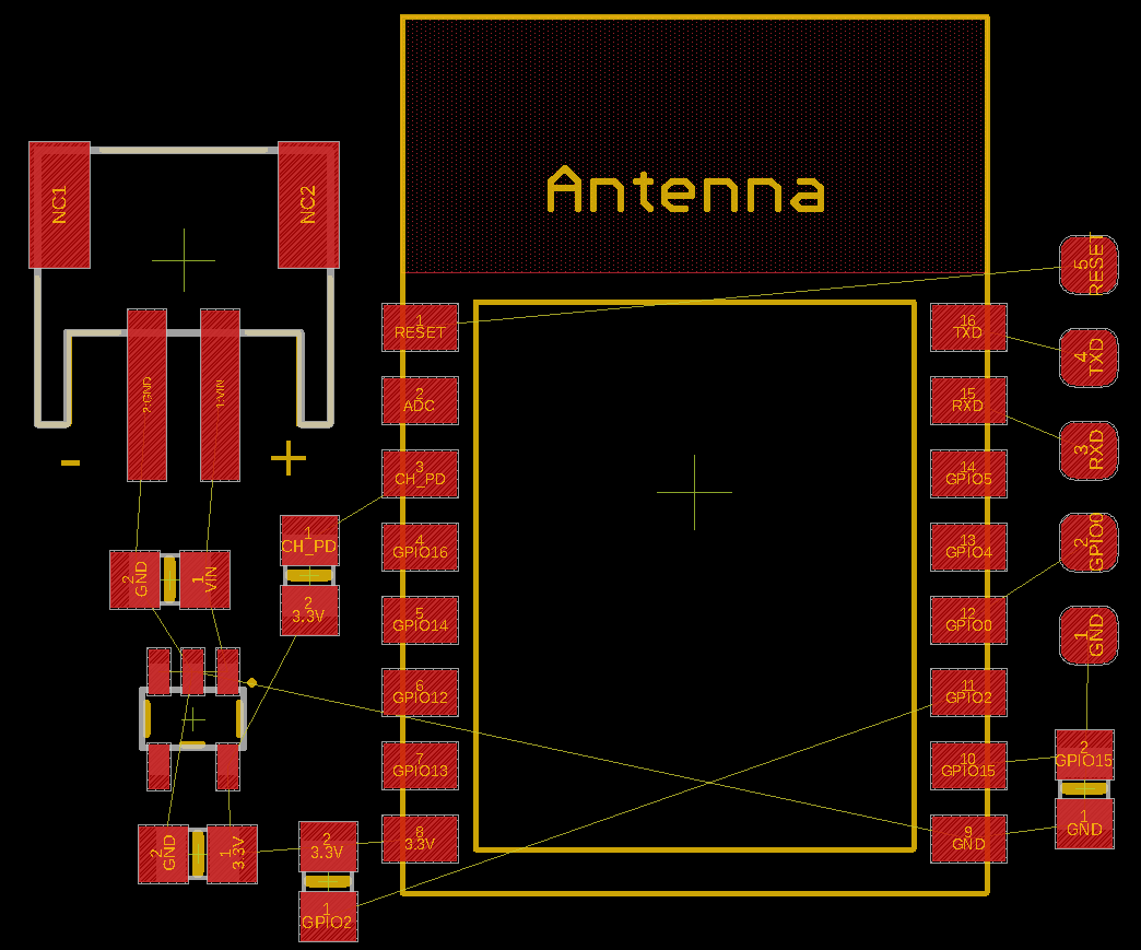
At the top left side of the schematic, there is a group of resistors, diodes, and buttons.
Let's go through them from left to right, and decide if we need them or not.
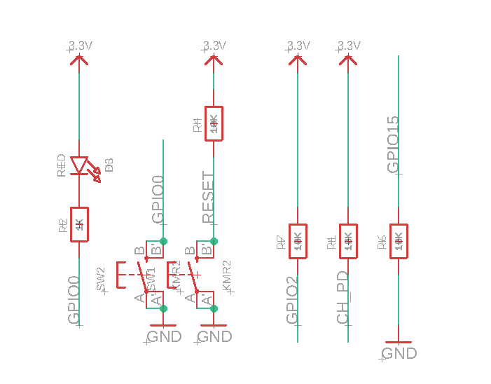
The LED on the left is connected to pin GPIO0. Because I want to start my design as simple as possible, I don't want to keep this LED around.
I decided to delete the LED.
Next, there are two buttons, one connecting GPIO0 to ground, and the other connecting RESET to ground. If you read through Adafruit's tutorial on uploading a blink sketch, these two pins are used to start the serial bootloader.
I will need buttons to program my final project, however I do not need to have those buttons on my PCB. For example, I can make a programming jig that holds those buttons.
I decided to delete the buttons.
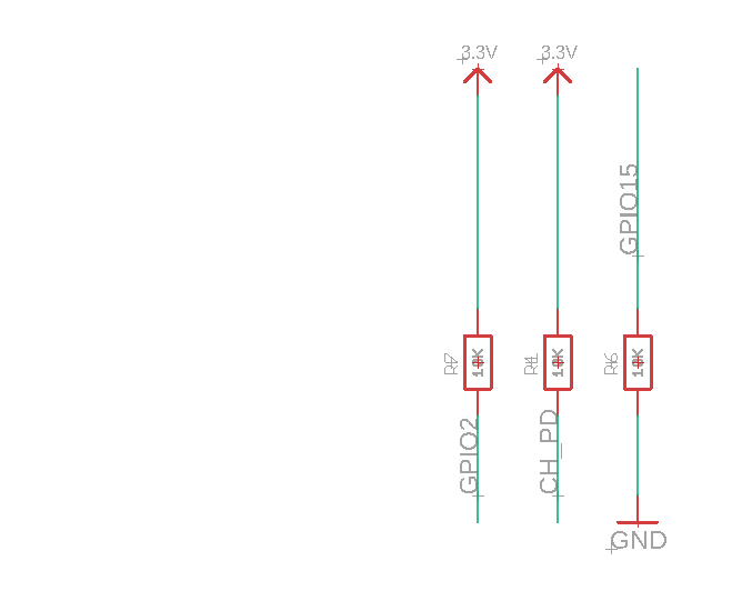
Finally, there are three resistors. They are "pulling-up" or "pulling-down" some of the ESP8266 pins. I don't see anything in Adafruit's tutorials about these pins, so these pins might be required for something that I do not know about. If I want to learn about the pins and what the resistors are doing, I could take the time to read the module's datasheet or it's shorter manual.
I decided to keep the resistors there.
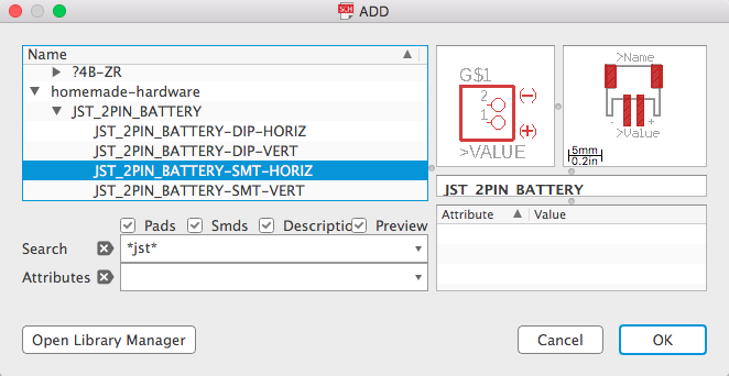
The last thing we need to add are the connectors. We need one connector for power, and another for the programming pins.
For power, I'll add a JST LiPo battery connector. The voltage coming from the battery we will connect to Vin.
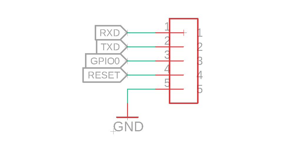
Finally, the programming pins need to include serial pins, ground, reset, and GPIO0.
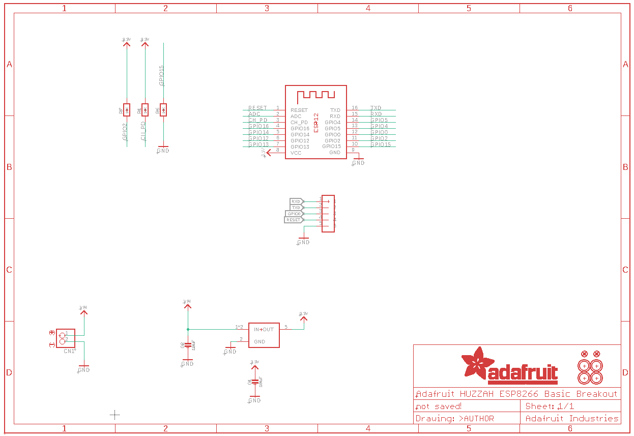
The ESP8266 schematic now looks like this.
The final step before saving this schematic is to delete all the extra labels the previous designer put on. This means, I want to delete the frame and the descriptions in the bottom right so they are no longer branded.
Also, it is hard to notice because they are just circles, but there are extra holes that Adafruit added to the board, hidden over there.
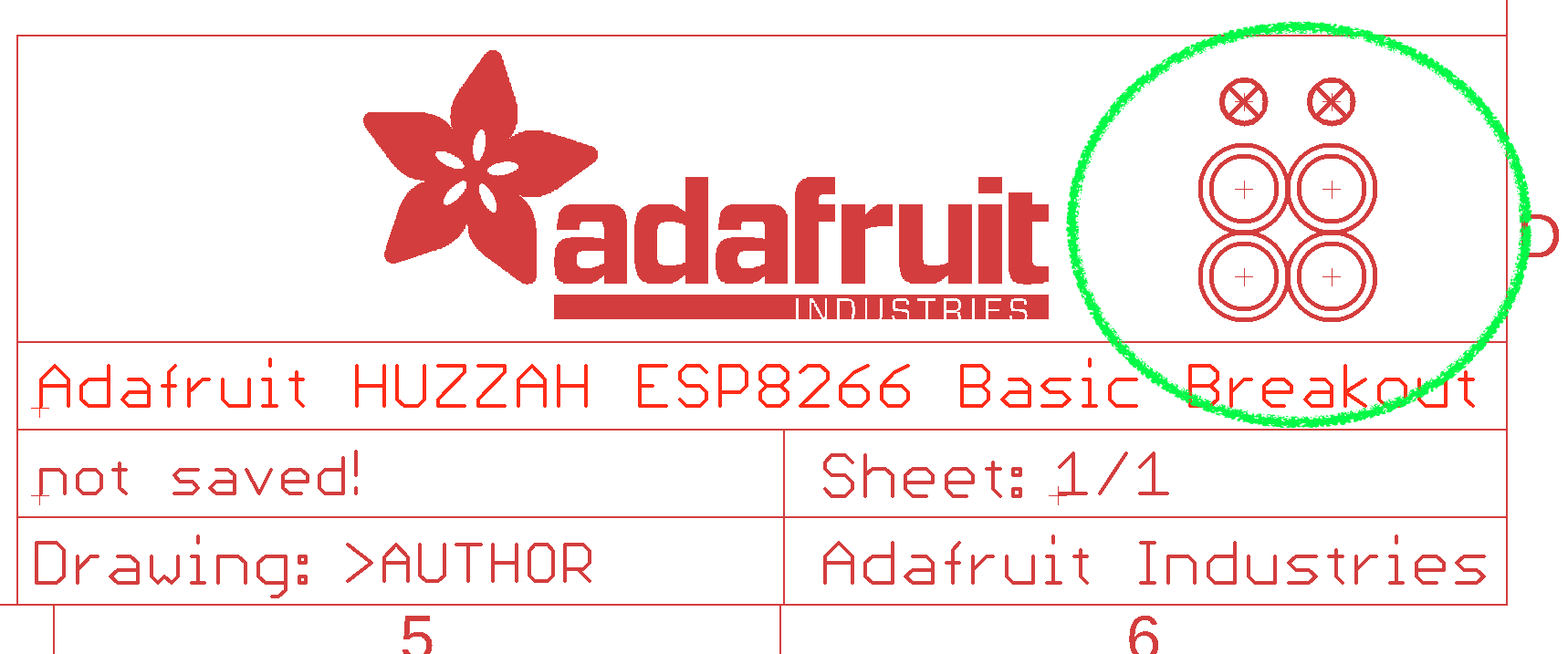
I am using the GROUP command to highlight and delete all of that.
And then I will add a new, plain frame with no branding (or holes) on it.
Change the Design Rules (DRC)
Go to the board design editor. Before I do anything here, I want to make sure the editor is setup for designing PCBs for the Bantam milling machine. That means that the route widths, hole sizes, and other defaults are set correctly.
To do this, you must load in the Bantam Design Rules Check (DRC).
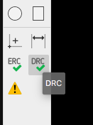
In the bottom left corner of the board design toolbar, you will see a button for DRC. Click it, and a window will open.
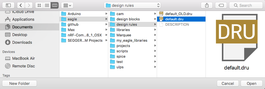
Reading the window, I can see that right now this design file is using an Adafruit DRC settings file. To change to a different file, press the Load... button.
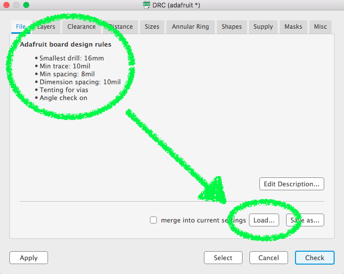
In the Documents->Eagle->design rules folder, select default.dru (which you should have edited in the Eagle Setup guide).
Now the DRC window will say that it is for the 1/32" endmill bit (perfect!).
Press the Apply button to save the changes, and then exit the window by pressing Cancel or the X on the window.
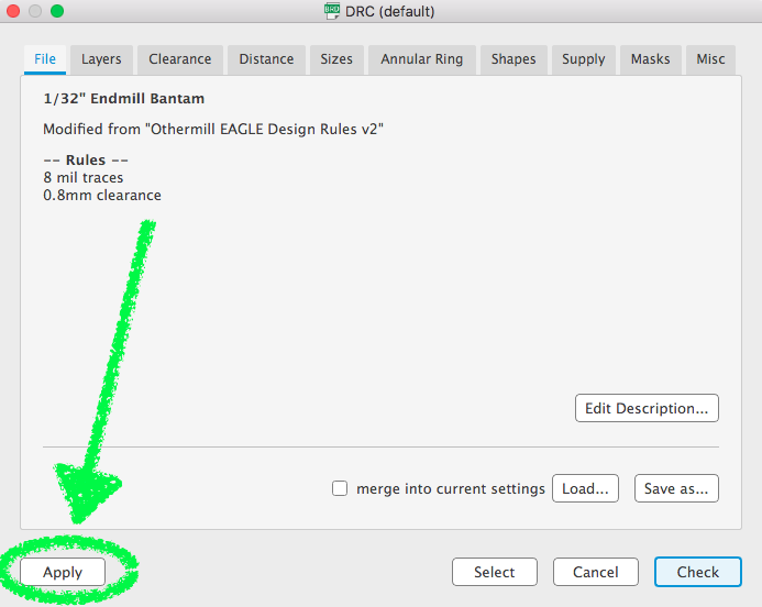
Now the design editor will set routes widthes, hole diameters, and other defaults to be good numbers for the Bantam milling machine (yay!).
Simplify the Board Design
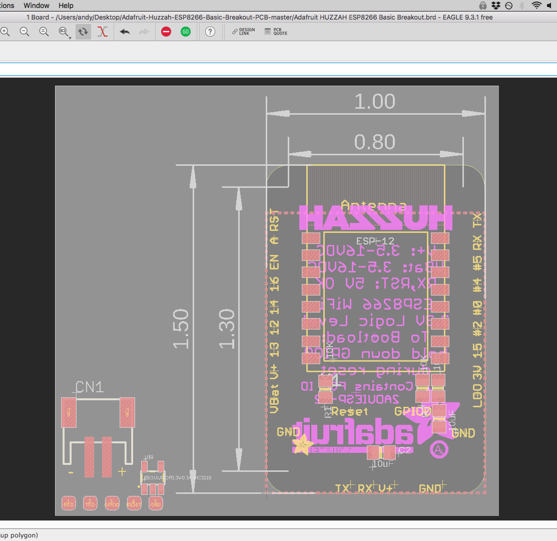
When I first move to the board design editor, it is a little messy. There are the new parts added, the old parts, and a lot of layers drawn by Adafruit.
The first thing I like to do is to erase everything that is not relevant to a PCB made on a milling machine. Makes working with the file simpler.
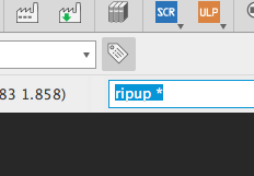
I'm going to first RIPUP all the routes, and then delete everything on the board (except the parts and connections).
In the command line input, enter ripup *. The asterisk means that all routes will be ripped up. Press ENTER to run the command.
Now all the small routes around the ESP8266 are gone, and replaced by the thin yellow unrouted lines.
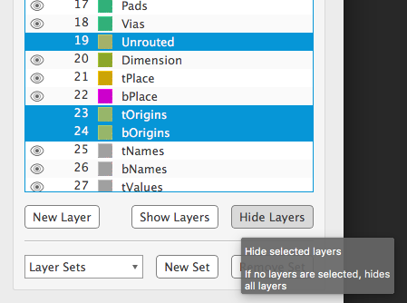
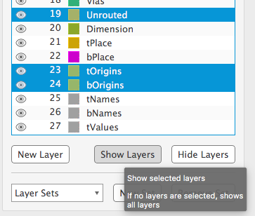
To prevent myself from deleting parts or connections, I'm going to hide the following layers:
- 19 Unrouted
- 23 tOrigins
- 24 bOrigins
Then, using the GROUP command, highlight everything in the file and delete them. Because the origin and unrouted layers are hiden, then will not be affected.
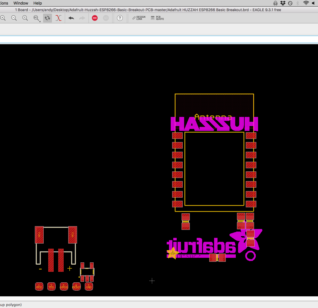
There are still some labels that Adafruit added on the design. I am going to show all the origin layers again. Once I can see the labels' origin crosses, I can zoom in and delete them.
Zoom in on the labels, find the origin cross for the label, and use the DELETE command.
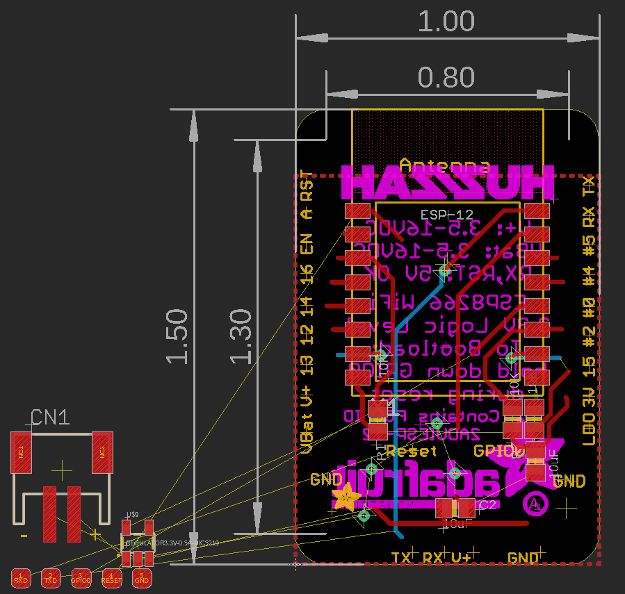
I moved the parts around, and now the simplified ESP8266 schematic now looks like this.
Check for Correct Packages
Before spending all that time routing a PCB, you should make sure the packages in your file are correct. That means, the parts are the same as the physical parts you will use.
When making PCBs, you need make absolute certain the packages are correct, or else the entire board could be a waste.
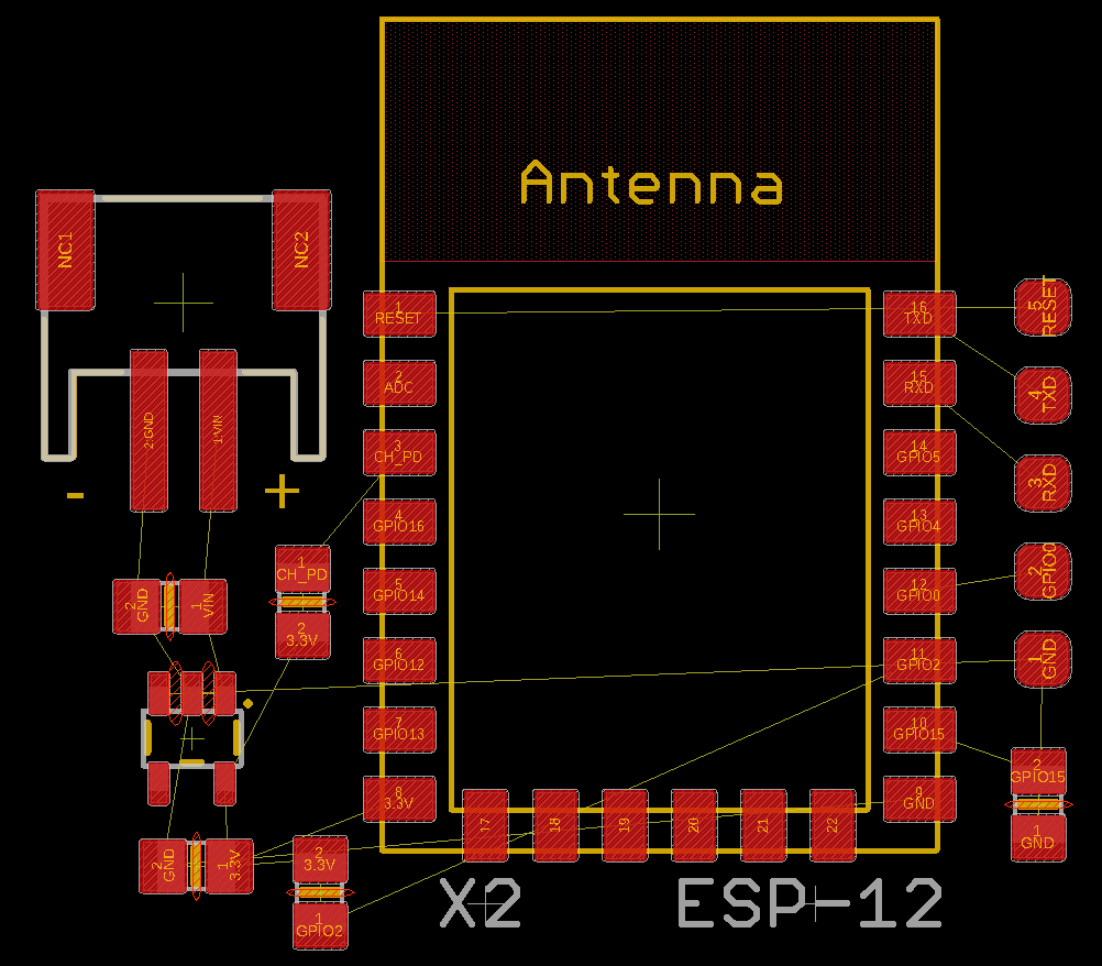
Below is a picture of the ESP8266 module I ordered. It is the module from Adafruit, however it is slightly different.
There are 6 new pins on the bottom.
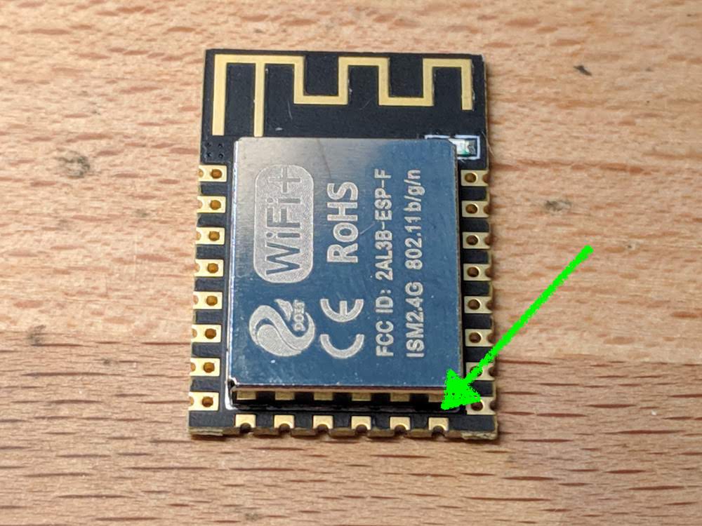
Now I have two options: 1) find a design online that has the correct package, or 2) add 6 new pins in Eagle Library editor.
I'm first going to try number one. Using the Library editor will come in a later tutorial.
Adafruit has more boards that use this module. The Feather PCB on Github has the package version with the added 6 pins. In the schematic, it is on the left side.
I'm going to copy/paste the schematic symbol from the Feather PCB to my PCB's schematic (copy/paste parts in board editor should not work).
NOTE: do not simply use the COPY command and then click the part. This will not copy the part to your computer's "clipboard". To copy to the clipboard, highlight the part with the
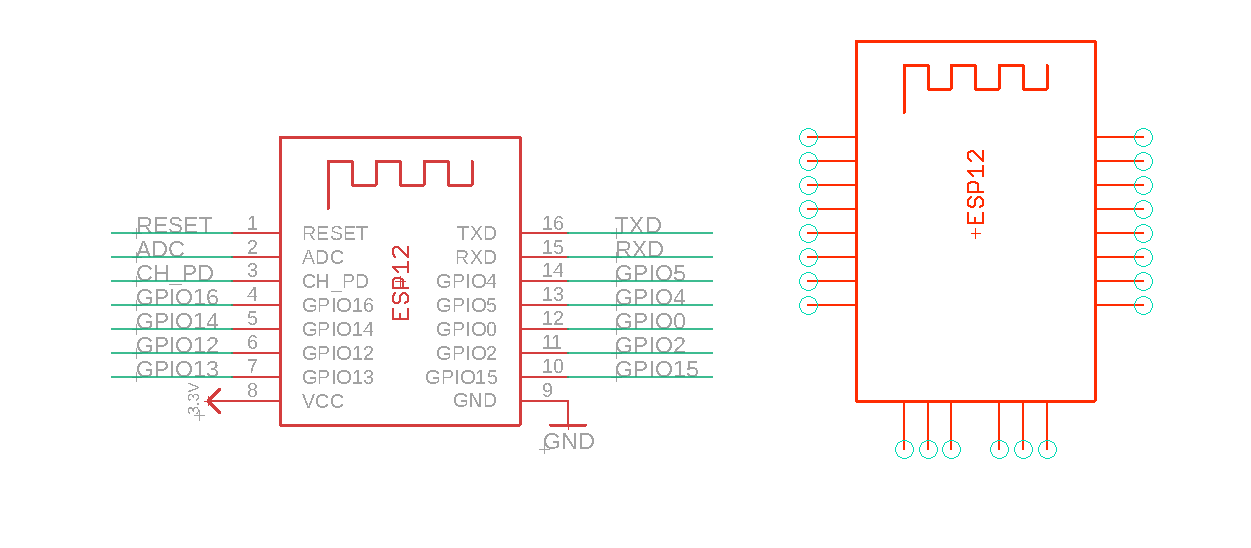
Luckily, all the pins on the new schematic symbol match the pins on the old schematic symbol. So I can simply delete the old one, and move the new one in it's same place with the green connections.
Now, switching back to my board design, I can see that all the packages on my PCB now match the parts I ordered (yay!).
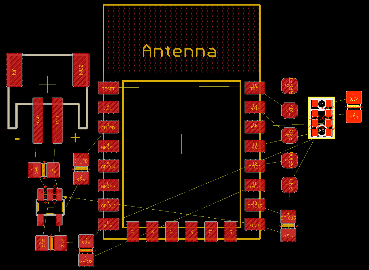
Combining Different Circuits
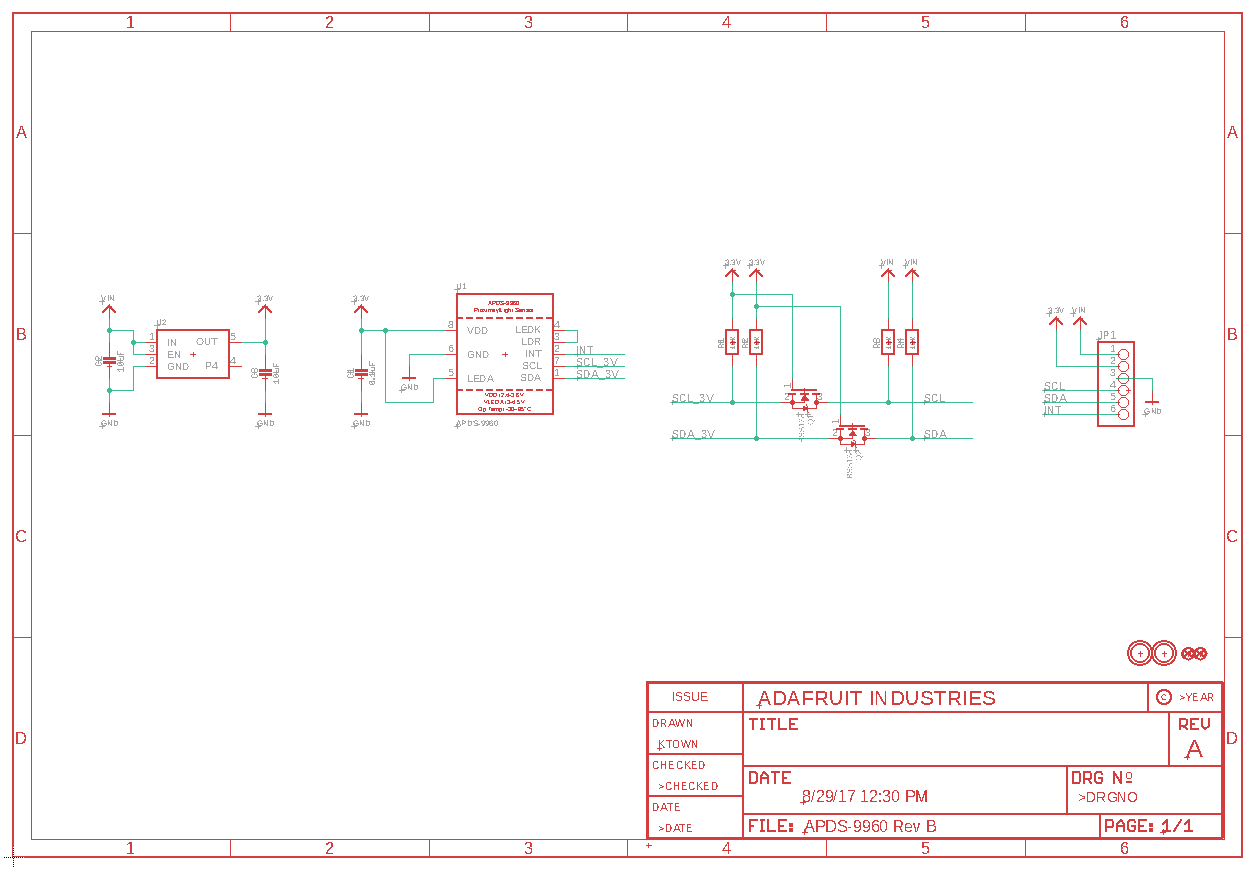
Now, I want to add a sensor to the PCB. I'll use the APDS9960, which I can also test out and breadboard with the breakout from Adafruit, and there design files are on Github.
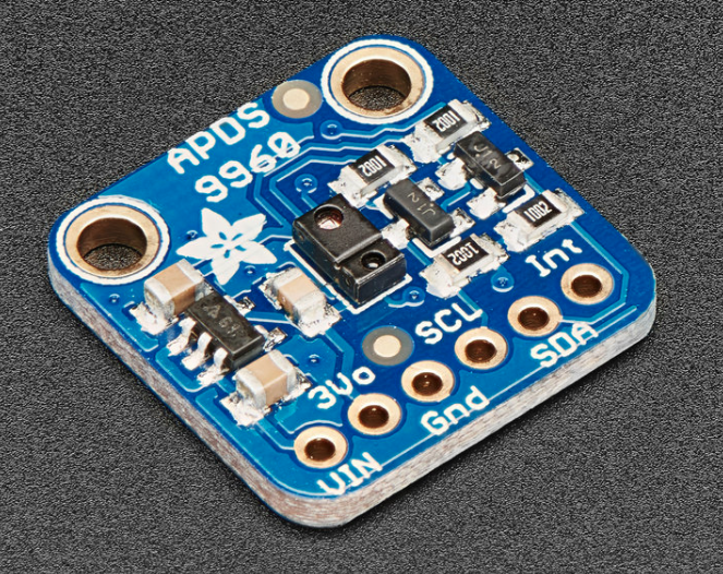
Just like before, I am going to first remove everything from the schematic that I do not need. The things I delete are:
- the 3.3 volt regulator (because my PCB already has one)
- the voltage protection transistors (because our PCB's voltage is a safe 3.3V)
- the headers (because our PCB is a contained project)
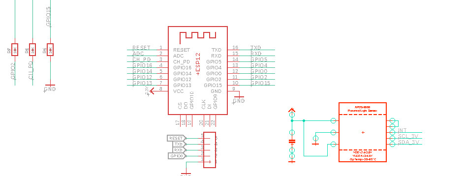
Before...
And after...
Now I am going to copy/paste that entire schematic into my PCB design file.
NOTE: do not simply use the COPY command and then click the part. This will not copy the part to your computer's "clipboard". To copy to the clipboard, highlight the part with the
Finally, connect the new parts to the rest of the schematic. For this circuit, I need to:
- Make sure my power (3.3V) and ground (GND) net names are all correct. For example, maybe you copied a Vcc named symbol, when the rest of the circuit is using a 3.3V named symbol.
- Connect the I2C data lines between the microcontroller and the sensor. These are SDA and SCL
Luckily for me, both the boards were originally designed by Adafruit, so all the power and ground symbols have the same names (3.3V and GND)
Adafruit's pinout description says that the I2C data lines on the ESP8266 are on pins 4 and 5. I'll connect those by giving them the same name, and a flag label.
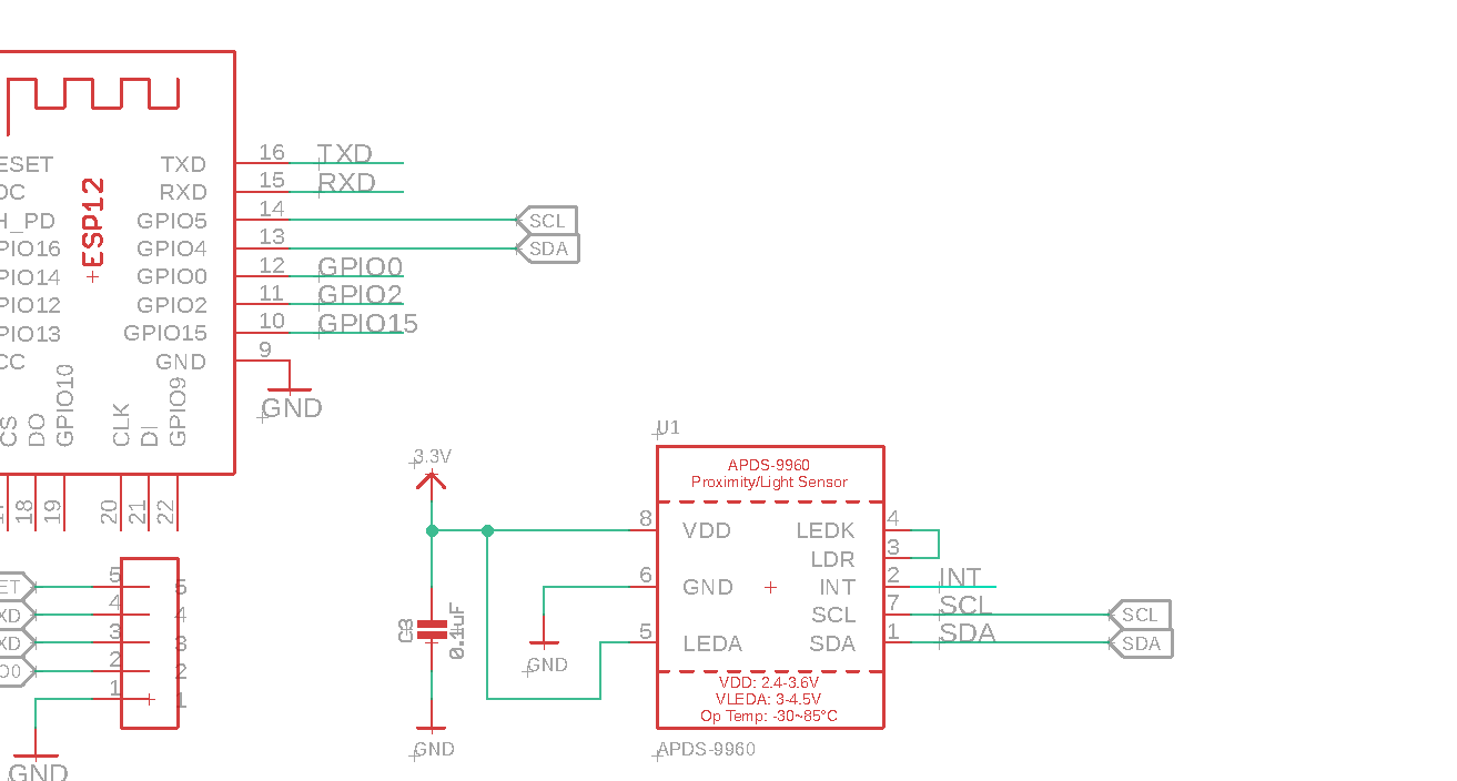
Now, going to the board designer and moving the sensor around, I have a final circuit for my WiFi connected, proximity sensing, battery powered PCB.
With the DRC loaded from before, all the routes and holes you draw will be able to be milled by the Bantam machine.